Sony and TSMC Are Spending Billions to Make Next-Gen Image Sensors
Our take
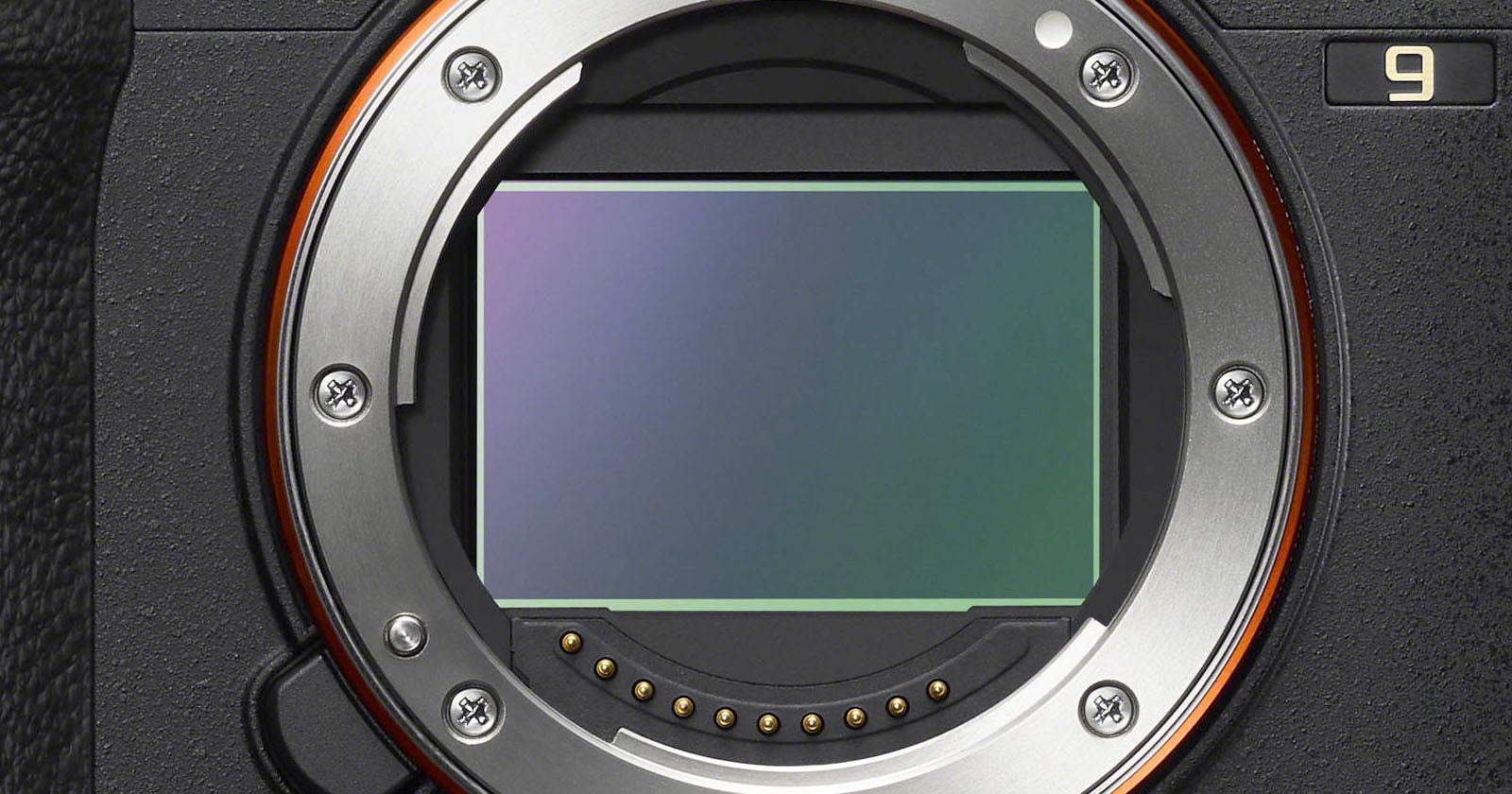
The announcement of Sony and TSMC’s joint venture to construct a next-generation image sensor fabrication facility in southwestern Japan signals a significant shift in the photographic landscape, one with implications far beyond simply improved camera resolution. This isn’t merely about sharper images; it’s about securing a critical supply chain and pushing the boundaries of what's possible in visual capture technology. Considering the recent challenges faced by lens manufacturers like Tamron, whose Tamron’s OEM Lens Sales Plummet As Company Considers Sony’s Takeover demonstrates vulnerabilities in a consolidating market, Sony’s move underscores a desire for greater vertical integration and control. The sheer scale of the investment—billions of dollars—reinforces this commitment, positioning Sony to potentially dominate the next era of image sensing. The rise of increasingly sophisticated and often budget-friendly action cameras and 360 cameras, exemplified by DJI’s ongoing innovations like the DJI Teases Osmo 360 II With Footage From the New Camera, further emphasizes the growing demand for advanced image sensors across a broad spectrum of devices.
The strategic location of the facility in Japan is also noteworthy. Bringing production back to Japanese soil mitigates geopolitical risks associated with reliance on overseas manufacturing and allows for closer collaboration between Sony’s design teams and the fabrication process. TSMC’s involvement is crucial; they are the undisputed leaders in semiconductor manufacturing, possessing the technological expertise to realize Sony’s ambitious designs. The timeframe—2029—suggests that these sensors will incorporate breakthroughs beyond current capabilities, likely leveraging advancements in materials science and potentially even quantum computing principles to achieve unprecedented levels of light sensitivity, dynamic range, and resolution. We've seen how innovative designs can sometimes struggle with real-world implementation, as evidenced by the mixed reception of devices like the Godox C100 Review: A Troubled Viewpoint, and Sony's partnership with TSMC aims to avoid those pitfalls. This collaboration promises a more refined and robust production process, ensuring that cutting-edge technology translates into reliable and high-performing sensors.
The implications extend beyond still photography and videography. Advanced image sensors are increasingly vital in automotive applications (ADAS, autonomous driving), medical imaging, industrial inspection, and even augmented and virtual reality. Sony’s investment isn’t solely about improving the cameras we use for personal enjoyment; it's about fueling innovation across numerous industries that rely on high-quality visual data. The development of these sensors will likely drive advancements in computational photography, enabling cameras to perform more sophisticated image processing tasks directly within the device, further blurring the lines between hardware and software. This shift will empower photographers and videographers to achieve creative effects previously requiring extensive post-production work. The resulting sensors will almost certainly reshape how we perceive and interact with the world, delivering richer, more detailed, and more accurate visual experiences.
Looking ahead, the most compelling question isn’t simply what these next-generation sensors will *do*, but how they will fundamentally alter the creative process. Will we see a rise in entirely new photographic genres enabled by these technologies? Will the ability to capture unprecedented levels of detail democratize professional-quality image creation, empowering a new generation of visual storytellers? And perhaps most importantly, will Sony's dominance in this space lead to further consolidation within the industry, or will it spur competition and innovation from other manufacturers seeking to challenge their position? The next few years promise a fascinating evolution in the world of image sensing, and Sony’s investment suggests a future where the boundaries of visual capture are continually redefined.
Sony Group and chip giant Taiwan Semiconductor Manufacturing Co. (TSMC) are planning to begin mass production of next-generation image sensors in southwestern Japan as soon as 2029, per Nikkei Asia.
Read on the original site
Open the publisher's page for the full experience